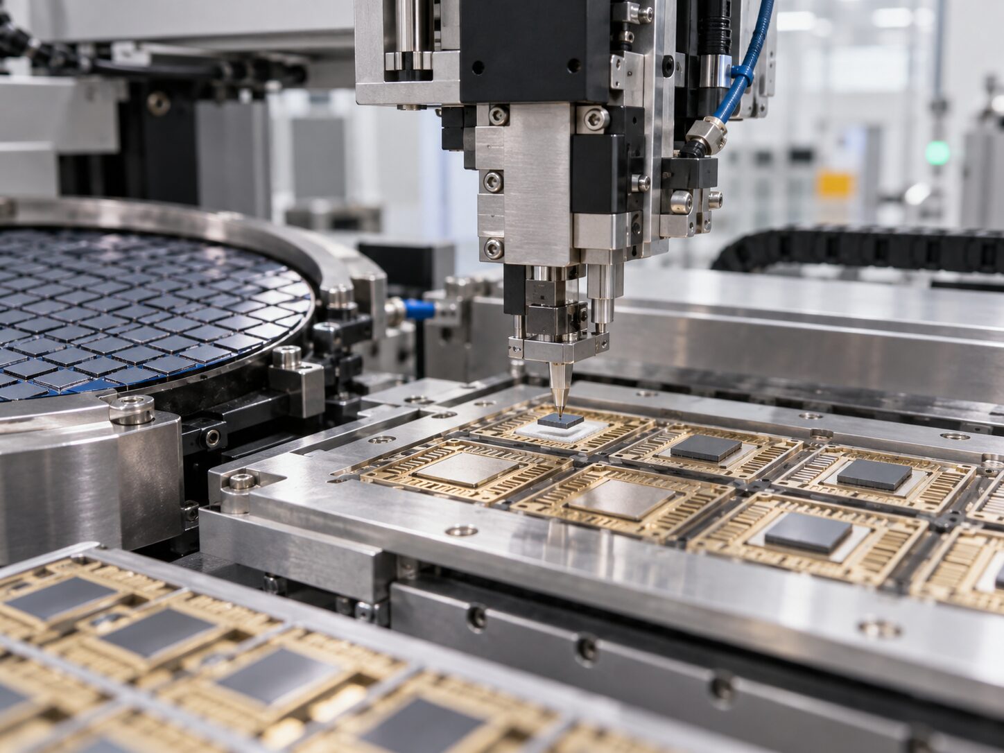
Semiconductor Application
Die Attach & Interconnects
High electrical and thermal conductivity at manufacturing compatible processing conditions.
Discuss your specification
Relevant Materials

Conductive metal nanoparticles

01

Nano Silver

Compared to microparticles, nano silver reduces the sintering temperature which increases application flexibility and protects temperature sensitive components during manufacturing. AM's platform produces spherical, cubic-phase Ag in the 1–100 nm range, directly relevant to conductive inks/pastes and technically applicable to sinter formulations.

02

Nano Copper

Copper is a significantly lower cost and more sustainable metal which typically oxidises quickly. AM's continuous microreactor platform enables high precision synthesis and encapsulation of nano copper to protect against degradation.

Why the attach layer matters

In semiconductor packages, the attach layer carries heat, current and mechanical stress

GPUs, Mobile Devices and Power Electronics can operate at high power density and elevated junction temperature, increasing the demands on the die-attach interface. The joint must combine low thermal and electrical resistance with mechanical integrity through thermal cycling and aging.

Silver sintering is an established high-performance route. Copper sintering is technically attractive because of conductivity and cost, but oxidation and surface control remain major development challenges. AM has demonstrated controlled silver particle synthesis, while copper represents an additional development route for applications that benefit from its conductivity and cost profile. The particle chemistry, oxidation control and sintering window can be engineered around the target package and process.
From powder to joint

A sintered interface is created in stages, and each stage has a particle-control consequence

Powder and paste state

Primary size, agglomerate size, surface chemistry and solids loading set the starting packing density and organic-removal requirement.

Print or dispense

Rheology and the coarse particle tail affect stencil release, dispense stability and bondline consistency.

Drying and debinding

Volatile removal must avoid skinning, large voids and uncontrolled particle redistribution.

Sintering and neck growth

Clean, reactive particle surfaces are needed for neck formation and densification. Cu adds the need for oxide management.

Joint microstructure

Residual porosity, interface contact and grain connectivity determine thermal resistance, electrical resistance and mechanical strength.
Conductive Inks, Pastes & Printed Electronics

From particle to printed conductor

A printed trace is the result of particle synthesis, formulation, deposition and cure acting together. Conductive inks and pastes must pass through a defined printing process, wet the substrate, dry without uncontrolled migration and form a continuous electrical network.

Particle size, surface chemistry and agglomeration influence every stage. AM positions the particle population as an input to the customer’s formulation and printing process, not as a guarantee that a powder specification alone delivers final conductivity.
Explore semiconductor materials
Specification Logic

Better particles specifications create better processes

Particle population

Primary size, D10/D50/D90, agglomerate tail and lot-to-lot distribution.

Morphology and packing

Spherical, flake or blended populations selected for packing, rheology and contact-network formation.

Surface condition

Organic coverage, oxide state, storage stability and compatibility with the sintering atmosphere.

Process compatibility

Stencil or dispense route, wet/final bondline, drying profile, peak temperature, pressure and surface finish.

Joint targets

Porosity, thermal/electrical performance, die shear and reliability after thermal cycling or aging.
The AM development route

Build the particle and sintering window around the joint you need, then preserve the formation logic as material demand increases

Using AM's material process library to quickly develop your own formulation

K1 · Particle and sinter window

For Ag, map synthesis conditions against particle size, morphology, surface state and early sinter performance. For Cu, first establish chemistry and oxidation-control feasibility.

K10 · Qualification material

Produce repeat lots for paste formulation, print/dispense trials, sinter optimisation and package reliability testing.

K100 · Production route

Increase output only after the qualified particle window and downstream process are established, maintaining the same continuous-flow logic.

Start with the package

Bring your specification

Useful inputs include die size and metallisation, substrate finish, target bondline, print or dispense method, available pressure, peak temperature, atmosphere, thermal/electrical targets, reliability plan and current paste or powder limitation.

Get in Touch

This field is for validation purposes and should be left unchanged.