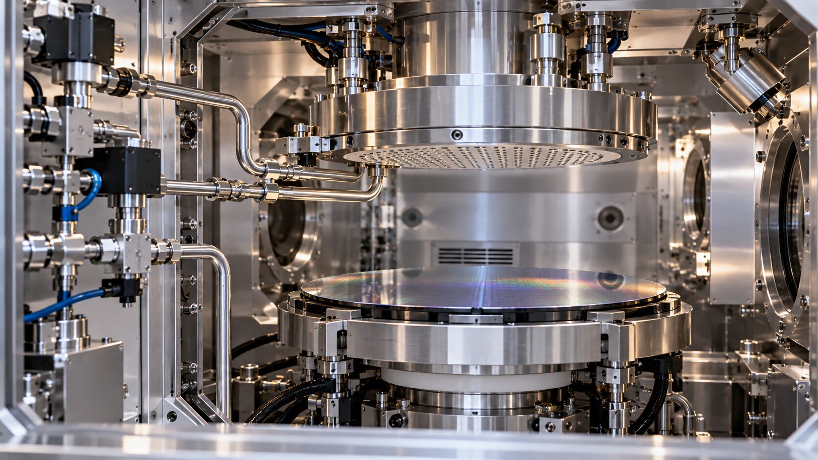
Semiconductor Applications
Front End Opportunities
Chemical Mechanical Polishing, Atomic Layer Deposition & Advanced Photoresist Select front end materials where controlled chemistry, particle formation and reproducible scale up add value.
Book a Semiconductor Materials Consultation
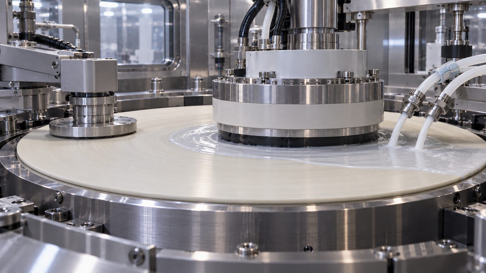

Material Requirements

Start with the process window

The required chemistry, purity, particle population and surface state are defined by the manufacturing step and downstream qualification route.

Process requirement: deposition · planarisation · patterning

Material controls: purity · particle size · agglomeration · surface chemistry · crystal phase

Development route: K1 · K10 · K100 · AMLearn
Explore semiconductor materials
Front End

CMP Slurry Components

Engineered oxide particles with tighter control over size, agglomeration and defect relevant tails

Front End

Photoresist & Lithography Materials

Engineered oxide particles with tighter control over size, agglomeration and defect relevant tails

Front End

ALD Related Materials

Specialist functional materials where controlled synthesis can support next generation patterning

Start with the process specification

Tell us the front end material requirement and qualification constraint

Share the process step, target material function, purity and contamination limits, current scale, required volume and the performance constraint that is preventing progress. AM can then assess where controlled synthesis, particle engineering and reproducible scale up can contribute.

Get in Touch

This field is for validation purposes and should be left unchanged.